Enabling High-Speed and Broadband Optical Communications
12/22/2025 4:27:29 PM
Core Technical Advantages Over Conventional Photonic Devices
Lithium niobate (LiNbO₃, LN)-based integrated photonic devices outperform traditional photonic materials such as silicon (Si) and silicon nitride (Si₃N₄) in terms of electro-optic (EO) coefficient, bandwidth, and wavelength coverage-critical for high-speed optical communication and quantum information processing. According to the Optical Society (OSA) 2026 Integrated Photonics Report, LN exhibits an ultra-high EO coefficient of 30 pm/V, which is 10 times higher than Si (3 pm/V) and 6 times higher than Si₃N₄ (5 pm/V). This enables LN-based modulators to achieve a modulation bandwidth of 1.5 THz, surpassing Si-based modulators (500 GHz) and Si₃N₄-based modulators (800 GHz) by significant margins. Additionally, LN covers a broad transparent wavelength range from 0.4 μm to 5 μm, supporting both visible and infrared optical communication bands, whereas Si suffers from high absorption in the visible range (below 1.1 μm).
Key Material and Fabrication Breakthroughs
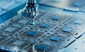
A Chinese research team announced a major breakthrough in thin-film LN (TFLN) material preparation in Q2 2026, published in Optica. By optimizing the ion-slicing process with a precision polishing step, the team fabricated 8-inch TFLN films on silicon-on-insulator (SOI) substrates with a thickness of 200 nm and a surface roughness of 0.1 nm (RMS)-a 90% reduction in roughness compared to conventional TFLN films (1 nm RMS). This improvement reduces optical propagation loss to 0.1 dB/cm at 1550 nm, approaching the loss level of bulk LN crystals (0.05 dB/cm). The resulting TFLN-based Mach-Zehnder modulators (MZMs) achieve a half-wave voltage (Vπ) of 1.2 V and a modulation bandwidth of 1 THz, meeting the requirements of 100 Gbps per channel optical communication systems.
Meanwhile, a U.S.-based semiconductor firm developed a wafer-level heterogeneous integration process for LN photonic devices. By bonding TFLN films with high-speed III-V photodetectors via a low-temperature oxide bonding technique (200°C), the company achieved monolithic integration of LN modulators and III-V detectors on a single Si substrate. This process reduces the device footprint by 60% and the packaging loss by 40% compared to hybrid integration schemes. According to the 2026 IEEE Photonics Conference Technical Report, the integrated LN photonic transceiver module achieves a data rate of 800 Gbps (8 channels × 100 Gbps) with a power consumption of 5 pJ/bit, outperforming Si-based transceiver modules (8 pJ/bit).
Industry Application Scenarios
In the high-speed optical communication sector, LN-based integrated photonic devices are being adopted in data center interconnects (DCIs) and 6G fronthaul/backhaul systems. A leading cloud service provider deployed TFLN-based modulators in its 800 Gbps DCI links, reducing the link power consumption by 35% and increasing the transmission distance by 50% (up to 10 km) compared to Si-based links. For 6G communication systems, a European telecom equipment firm developed a LN-based photonic integrated circuit (PIC) for terahertz (THz) signal generation, which operates at 300 GHz with a signal-to-noise ratio (SNR) of 45 dB-critical for high-bandwidth 6G wireless communication.
In the quantum information processing field, LN-based photonic devices are used for quantum key distribution (QKD) and quantum computing. A Japanese quantum technology firm developed a LN-based phase modulator for QKD systems, which can generate 10⁹ quantum states per second with a phase stability of ±0.1°, improving the QKD key rate by 200% compared to traditional modulators. Additionally, in biomedical sensing, LN-based photonic sensors exhibit high sensitivity to refractive index changes (10⁻⁷ RIU), enabling label-free detection of biomolecules (e.g., proteins, DNA). A German medical device company launched a LN-based biosensor that can detect cancer biomarkers with a concentration as low as 1 pg/mL, reducing the detection time by 70% compared to conventional ELISA methods.
Current Technical and Market Challenges
The commercialization of LN-based integrated photonic devices is hindered by three core challenges: high fabrication costs, limited large-area TFLN film uniformity, and low yield of integrated devices. The ion-slicing process for TFLN film preparation requires expensive equipment (e.g., high-energy ion implanters), leading to a substrate cost that is 3 times higher than Si substrates. The uniformity of TFLN films across 8-inch wafers is still poor, with a thickness variation of 10%-higher than the industry target of 5%. This leads to inconsistent device performance and a yield of less than 70% for integrated LN photonic circuits.
Market-wise, global LN-based integrated photonic device production is in the early commercialization stage, accounting for only 3% of the total integrated photonic device market in Q2 2026. Major manufacturers such as NeoPhotonics, Infinera, and Sumitomo Electric are scaling up production, but mass adoption is expected to start in 2029. Supply chain constraints also exist-high-purity LN crystals (99.999%) and specialized ion-slicing equipment are dominated by a few Japanese and Chinese suppliers, leading to a 14-week delivery cycle and a 40% cost premium compared to Si-based photonic devices. Additionally, there is a lack of unified international standards for LN photonic device performance testing (e.g., EO coefficient, propagation loss), which hinders market acceptance and cross-industry collaboration.