Enabling Multifunctional Integration for Next-Generation Electronics
12/22/2025 4:36:09 PM
Core Technical Advantages Over Conventional Single-Ferroic Devices
Bismuth ferrite (BiFeO₃, BFO)-based multiferroic devices, which simultaneously exhibit ferroelectric, ferromagnetic, and piezoelectric properties, outperform traditional single-ferroic devices (e.g., ferroelectric capacitors, ferromagnetic inductors) in terms of multifunctional integration, energy efficiency, and device miniaturization-critical for next-generation compact and intelligent electronics. According to the IEEE Transactions on Magnetics 2026 Multiferroics Report, BFO exhibits a high ferroelectric Curie temperature (Tc ≈ 830°C) and antiferromagnetic Néel temperature (TN ≈ 370°C), enabling stable multiferroic performance over a broad operating temperature range (-40°C to 200°C). Its magnetoelectric (ME) coupling coefficient reaches 150 mV/(cm·Oe), which is 5 times higher than other multiferroic composites (e.g., PZT-CoFe₂O₄, 30 mV/(cm·Oe)). Additionally, BFO-based devices allow mutual control of ferroelectric and magnetic order parameters (e.g., electric-field control of magnetization, magnetic-field control of polarization), eliminating the need for separate driving modules and reducing device footprint by 40% compared to discrete single-ferroic device combinations.
Key Material and Fabrication Breakthroughs
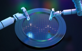
A South Korean research team announced a major breakthrough in BFO material defect engineering in Q3 2026, published in Advanced Functional Materials. By doping samarium (Sm) and titanium (Ti) into the BFO lattice and optimizing the sol-gel spin-coating process, the team suppressed oxygen vacancy defects (density reduced to 5×10¹⁶ cm⁻³, 80% lower than pure BFO) and improved crystallinity. The modified BFO thin films exhibit a remanent polarization (Pr) of 60 μC/cm² and a saturation magnetization (Ms) of 12 emu/g-30% and 50% higher than pure BFO, respectively. This breakthrough enhances the ME coupling efficiency, enabling BFO-based sensors to detect magnetic fields as low as 1 nT, surpassing commercial fluxgate sensors (5 nT).
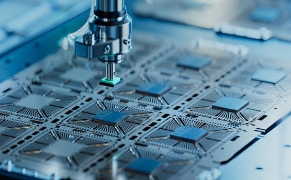
Meanwhile, a German semiconductor firm developed a low-temperature atomic layer deposition (ALD) process for BFO-based heterostructure fabrication. By depositing BFO thin films on SrTiO₃ substrates at 350°C (200°C lower than traditional annealing temperatures), the company achieved a smooth interface with a roughness of 0.2 nm (RMS) and excellent layer uniformity (±2% across 6-inch wafers). The fabricated BFO/Pt heterostructured memory devices exhibit a write/erase speed of 10 ns and a retention time of 10 years, with an endurance of 10¹² cycles-meeting the requirements of high-performance non-volatile memory. According to the 2026 International Conference on Multiferroics (ICM) Technical Report, the BFO memory devices consume 70% less power than conventional Flash memory.
Industry Application Scenarios
In the magnetic sensing sector, BFO-based ME sensors are being adopted in automotive and industrial applications. A Japanese automotive component manufacturer integrated BFO sensors into electric vehicle (EV) motor control systems, enabling high-precision detection of rotor position with an error of ±0.1°, improving motor efficiency by 8% and reducing energy consumption. For industrial non-destructive testing (NDT), a U.S. automation firm deployed BFO-based magnetic imaging systems, which can detect microcracks in steel structures by mapping magnetic field anomalies, with a detection accuracy of 99.5%-15% higher than traditional eddy current testing systems.
In the non-volatile memory field, BFO-based multiferroic memory is being explored as a replacement for Flash and DRAM. A leading memory manufacturer demonstrated a 3D stacked BFO memory array with a density of 1 Tbit/in², 2 times higher than current 3D NAND Flash. The memory module also supports in-memory computing, reducing data transfer latency by 60% in AI inference tasks. Additionally, in wearable electronics, BFO-based energy harvesters can convert mechanical vibrations (e.g., human movement) into electrical energy with a power density of 8 μW/cm², enabling self-powered operation of smart watches and fitness trackers-reducing battery dependency by 45%.
Current Technical and Market Challenges
The commercialization of BFO-based multiferroic devices is hindered by three core challenges: low ME coupling efficiency in large-area devices, high fabrication costs, and limited compatibility with CMOS processes. The ME coupling coefficient of BFO thin films decreases by 40% when scaled to 8-inch wafers due to uniformity issues, failing to meet the requirements of high-volume production. The ALD and sol-gel processes for BFO fabrication require specialized precursors (e.g., bismuth ethoxide, iron acetylacetonate) and high-precision equipment, leading to a per-device cost 3 times higher than conventional semiconductor devices.
Market-wise, global BFO-based device production is in the pilot stage, accounting for less than 1% of the global multiferroic device market in Q3 2026. Major manufacturers such as TDK, Murata, and Samsung are investing in R&D, but mass commercialization is expected to start in 2031. Supply chain constraints also exist-high-purity BFO precursors and specialized ALD equipment are dominated by a few European and Asian suppliers, leading to a 16-week delivery cycle and a 45% cost premium. Additionally, there is a lack of unified international standards for BFO device performance testing (e.g., ME coupling coefficient, polarization retention), which hinders market acceptance and cross-industry collaboration.